Utz Brands began trading under the symbol UTZ on the NYSE; Dylan Lissette joins Cheryl Casone with insight on 'The Claman Countdown.'
After seeing his company's stock soar more than 12% Monday when it began trading, Utz Brands CEO Dylan Lissette said the company’s plan to go public was in the works long before special purpose acquisition companies became a hot trend on Wall Street.
Continue Reading Below
Best known for its potato chips, the venerable snack brand held its first day of public trading on Monday following a reverse merger with Collier Creek Holdings, a SPAC co-founded by former Kraft Foods CEO Roger Deromedi. Lissette said the involvement of executives with proven track records such as Deromedi, who became chairman of Utz Brands, was a critical factor in the family-owned company’s decision to go public.
“What we really liked about it were the people and the game plan that they had executed in the past and how that might add value to our company,” Lissette said during an appearance on FOX Business Network.
SPACs have gained popularity on Wall Street in recent months as a means of taking a company public without the traditional initial public offering process. Sports betting firm DraftKings began public trading through a reverse merger earlier this year.
SPACs raise money through an IPO and then use the proceeds to fund mergers with companies looking to go public. Collier Creek held its IPO in 2018 at $10 per share.
Utz's stock opened at $18.95, up from Collier Creek's last close of $16.34 last Friday and closed at $18.40 on Monday -- good for a 12.61% gain for the day. The company expects to generate net sales of $932 million this year.
The Rice and Lissette families, the longtime owners of Utz Brands, still own more than 50 percent of the company. Lissette said the families’ continued involvement should give investors confidence about the company’s long-term direction.
“For someone who’s looking at investing in the brand, I would feel very comfortable and very happy to know that we’re retaining such a large stake in the company so that we can continue the magic that we’ve really worked on for just short of the last 100 years,” Lissette said.
Lissette said Utz took immediate steps to alter its operations when the coronavirus pandemic hit in March, with an emphasis on workplace safety measures such as social distancing and personal protective equipment. The company has operated during the pandemic without a major impact to its business.
As most dieters tend to cut calories in order to lose weight, manufacturers have come up with various lower-calorie substitutes of our favorite high-fat food.
A recent study, published in the Journal of Marketing Research, examines the perceptions behind these “diet” options and how we make our food choices, particularly when it comes to restrained eating.
The research found that people who frequently try to cut back on their eating tend to buy a large portion of a “light” substitute of high-calorie food, rather than a smaller package of their favorite indulgent foods.
Participants who indicated that they rarely dieted had the opposite preference, systematically picking out a smaller portion of high-calorie food like potato chips and candy.
These findings prompted researchers to conclude that a larger, “lighter” version of an indulgent food is perceived as healthier and more filling than the smaller, higher-caloric-density version of the same product.
Researchers have conducted a series of studies to assess how dietary restraint affects the trade-off between caloric density and portion size for consumers.
In one of them, participants were asked to choose between a medium-sized bag of Lay’s baked low-fat BBQ potato chips and a smaller package of the regular version, both of which have similar total calories.
Most chronic dieters, who often cut back on their eating by skipping meals or eating smaller servings, opted for the larger bag of “light” baked chips, while unrestrained eaters preferred the smaller package of regular Lays BBQ chips.
Similar experiences were conducted with other high-calorie snacks such as popcorn, cookies, macaroni and cheese and mayonnaise — all of which produced similar results.
Additionally, researchers noticed that “the larger but lower-caloric-density option was perceived as healthier and more filling, but less tasty than the smaller but higher caloric density option.”
“Small packages are less likely to be appealing to restrained eaters when positioned as targeted solutions to cut calories. By contrast, unrestrained eaters are likely less concerned with the ability of smaller packages of indulgent foods to be filling, and thus such small packages of indulgent foods may be targeted at unrestrained eaters who want to cut back or just want smaller servings,” researchers Peggy J. Liu and Kelly L. Haws wrote in the paper.
“Low-fat” doesn’t necessarily equate to fewer calories
Researchers have long been studying the impact of packaged low-fat snacks on normal-weight and overweight people.
A study, conducted in 2006 by researchers at Cornell University, showed that overweight people consume up to 50 percent more calories when they eat “diet” versions of snack foods than when they eat the regular versions.
At the time, researchers also found that many low-fat-labeled foods have only about 30 percent fewer calories than their regular counterparts.
“Low-fat labels trick people into eating more than regular labels. But the cruel twist is that these labels have an even more dramatic impact on those who are overweight. They are at danger for really overindulging when they see something with a low-fat label. If we are looking for an excuse to eat, low-fat labels give it to us,” said Brian Wansink, the John S. Dyson Professor of Marketing and of Applied Economics at Cornell.
Taiwan Semiconductor Manufacturing Co. (TSMC) recently shared some details about its progress and plans for the coming years.
TSMC will continue to introduce new leading-edge manufacturing processes annually; 5nm chips this year and 3nm processors in late 2022.
For customers that need more than a leading-edge node, meanwhile, TSMC will offer new packaging technologies that will enable to create ultra-compact SiPs, as well as behemoth-sized SoCs for supercomputers.
TSMC: a $400 billion company
There are only a few companies in the world with leading-edge process technologies that can be used to build highly-complex processors for datacenters and supercomputers, GPUs, and smartphone SoCs. Intel and Samsung Electronics are integrated device manufacturers (IDMs) that are focused on both chip design and process nodes. By contrast, TSMC is a pureplay foundry that is focused on production and nothing else.
Valued at nearly $400 billion (as of late August, 2020), TSMC is the world’s largest contract maker of semiconductors that produces some of the most advanced chips today, for companies like Apple, AMD, Nvidia, and Intel. To a large degree, TSMC’s process technologies and capabilities define what its clients will be able to offer, so it is important to watch TSMC and its plans closely.
TSMC recently held its annual Technology Symposium where it revealed details about its progress with its current and future leading-edge nodes, as well as many other important factors for the future of chips.
TSMC N5: in production with good yields
TSMC confirmed that it had started high volume production of chips using its N5 (5nm) process technology earlier this year. According to the world’s leading contract maker of semiconductors, the new process has lower defect densities than the previous generation node at the same time of its lifespan, which is a positive news for TSMC clients.
(Image credit: TSMC)
When compared to TSMC’s N7 process technology (which is used to make AMD’s latest Epyc and Ryzen 3000/4000-series CPUs), the company’s N5 node promises to increase performance by up to 15% at the same power, or reduce power consumption by up to 30% at the same clocks and complexity.
Further, transistor density of TSMC’s N5 is up to 1.8x higher than that of N7, but not at all transistor structures. For fabless chip designers, these improvements mean ability to meaningfully boost frequencies of their chips as well as add features due to higher transistor budgets.
TSMC’s 5nm process technology extensively uses extreme ultraviolet (EUV) lithography on 10+ layers to reduce mask count to 81 and avoid usage of multipatterning where possible, which optimizes costs and may improve yields.
TSMC says that its 5nm fabrication process has significantly lower defect density when compared to 7nm early in its lifecycle. This means that current yields of 5nm chips are higher than yields of 7nm chips two years ago. Still, it will take N5 some time to get where N7 is today.
As a rule, TSMC does not disclose which of its customers are using its latest nodes, but AMD has already confirmed plans to use TSMC’s N5 process technology and Apple is also likely to use N5.
TSMC N5P: on track for next year, 10% higher performance
Next year TSMC plans to introduce a performance-enhanced version of the N5 process called N5P, which promises to boost frequencies by up to 5% or reduce power consumption by up to 10%.
TSMC’s N5 and N5P nodes are very similar, so almost any design implemented using the former can be quickly adopted for the latter for performance or power gains. Not all N5 customers are going to use N5P, but some of them might.
TSMC N4: due in 2022, easy to implement
TSMC’s N5 is the so-called long node that is set to be used and evolve for years to come. The next step in N5’s program is called N4, which is expected to enter risk production in Q4 2021 and volume production sometimes in 2022.
(Image credit: TSMC)
TSMC’s 4nm process technology will extend usage of EUV lithography tools, which will allow the firm to reduce masks count and costs further. The company has not disclosed any information about expected improvements, but N4 expected to be good enough to motivate customers to use the technology.
One of the most important aspects of N4 is that it features N5-compatible design rules, SPICE (simulation program with integrated circuit emphasis) models and IP. To that end, it will be very easy for SoC developers with 5nm designs to adopt TSMC’s 4nm technology and even re-use some of the building blocks they already have.
TSMC N3: significant improvements for upcoming chips
TSMC’s N3 manufacturing technology will be a brand-new node that promises to bring substantial transistor density improvements for high-end processors designed by companies like Apple, AMD, and Nvidia as well as various emerging players working on specialized AI SoCs.
(Image credit: TSMC)
When compared to TSMC’s existing N5 manufacturing process, the new N3 technology promises to increase performance by 10% – 15% (at the same power) or cut power consumption by 25% – 30% (at the same performance), and improve transistor density by up to 1.7 times for some logic structures, up to 1.2 times for SRAM cells, and only up to 1.1 times for analog structures.
It should be noted that not all N3 structures are set to shrink by up to 1.7 times when compared to N5, so actual chip level transistor density improvement may be around 33%. Meanwhile, even a 33% transistor density increase represents a significant advantage for complex chips, such as CPUs, GPUs, and mobile SoCs.
The new node will use both deep-ultraviolet (DUV) and extreme-ultraviolet (EUV) lithography, but it is reasonable to expect usage of EUV to increase, which is what enables performance/power and transistor density improvements.
TSMC plans to start high-volume production (HVM) of chips using its N3 fabrication technology sometimes in the second half of 2022.
TSMC N3: play it safe with FinFETs
TSMC’s N3 technology will continue to use FinFET technology, the same transistor structure used today. By contrast, Samsung Foundry will switch to gate-all-around (GAAFET) transistor structure with its 3nm process, in a bid to get a substantial generation-to-generation performance and power efficiency gain.
(Image credit: TSMC)
TSMC decided to retain the existing type of transistors for N3 to ensure the technology is rolled out on schedule.
GAAFETs (also known as stacked carbon nanosheets/nanowires) have numerous advantages, but they are harder to produce. Further, usage of new transistor structures requires a whole new stack of electronic design automation (EDA) tools and necessitates development of all-new IP. Ultimately, the switch to GAAFETs may increase design costs, just like switch to FinFETs back in 2014/2015.
So, to play it safe and ensure high initial yields, as well as make life of its customers a bit easier, keeping FinFETs for N3 makes sense. In the end, FinFET structures can be optimized in dozens of ways to extract additional performance, power, and transistor density.
Beyond N3: GAAFETs, new materials
Not using GAAFETs for 3nm does not mean that TSMC does not work on this new transistor structure like other companies do. The contract maker has experimented with GAAFETs for 15 years, so commercial implementation of the technology at a cadence different from a rival is neither good nor bad.
(Image credit: TSMC)
TSMC has demonstrated working 32Mb nanosheet SRAMs at 0.46V with good characteristics. But the company believes that its post-N3 nodes will need more than just a new transistor structure, but will also need new materials that will be good enough for years to come (i.e. TSMC can improve structures without completely changing materials) and improvements to other parts of the chip.
(Image credit: TSMC)
TSMC 3DFabric: enabling skyscraper and behemoth chips
Leading-edge and specialty process technologies allow to build the right silicon using the right methods, but sometimes capabilities of nodes are not enough. This is where TSMC’s comprehensive family of 3D/2.5D silicon stacking and advanced packaging technologies comes in.
(Image credit: TSMC)
TSMC’s 3DFabric family of technologies includes 2D and 3D frontend and backend interconnect technologies. The frontend subfamily includes such 3D solutions as Chip-on-Wafer (CoW) and Wafer-on-Wafer (WoW) that allow to precisely stack similar and dissimilar dies. The backend subfamily includes well-known Chip-on-Wafer-on-Substrate (CoWoS) and InFO packaging technologies.
At its Technology Symposium, TSMC demonstrated how it can build a 12-Hi CoW design with a 600µm thickness using through silicon vias (TSVs). This ‘skyscraper’ technology enables to stack up to 12 chips together to get extra performance with additional compute dies, add HBM memory or NAND storage, or improve power delivery with deep trench capacitors, all on a very small footprint. Such advanced system-in-packages (SiPs) might enable applications not possible today.
(Image credit: TSMC)
The AI megatrend drives demand for chip performance at a rather rapid pace, but at the same time, transistor shrinks are slowing down. To that end, there is a growing interest in building large chips in general - and chips larger than the reticle size of a lithography machine in particular.
For example, the reticle size of today’s DUV and EUV scanners is 26 mm by 33 mm, or 858 mm². This defines the maximum size of a chip, or a chip with HBM2E memory on an interposer. To make something larger, chip-sticking (or rather interposer-sticking, to be more precise) technologies like CoWoS are needed.
Last year, TSMC built a 1,700mm² solution for Broadcom using two 5nm dies. At the Technology Symposium, TSMC showcased its CoWoS roadmap that shows 3X reticle-sized CoWoS-enabled assemblies in 2021, as well as a 4X reticle-size CoWoS assemblies in 2023.
(Image credit: TSMC)
The behemoth-sized 4X reticle chip assembly will feature a whopping size of around 3,400mm² - the size of a small chocolate bar.
Considering architectural and node-related improvements expected by 2023, it is fair to expect such behemoth multi-die chips to offer 6X – 7X peak theoretical performance of today’s flagship solutions. How about GPUs with a whopping 126 FP32 TFLOPS compute horsepower (A100 x6.5) three or four years from now?
To enable such massive theoretical performance, each 4X chip assembly will be equipped with 12 HBM2 memory stacks, which means a 12,228-bit bus. Even using currently available SK Hynix’s HBM2E 3600MT/s memory chips, that translates into an incredible 5.53TB/s memory bandwidth.
Summary
Having landed orders from the world’s leading chip designers, TSMC must introduce new process technologies every year to enable improvements of its clients’ processors on an annual cadence. This is exactly what TSMC promises with its leading-edge technologies in the next three or four years.
For those who need to build specialized highly-integrated solutions, TSMC continues to advance its 3DFabric family of packaging technologies.
Potato chip maker Utz Brands went public Monday after 99 years in business.
"This was a great time to go public," CEO Dylan Lissette told Cheddar. "We've been around for almost a hundred years. It's a fourth generation business that was transferring into the fifth generation. We were approaching about a billion dollars in sales."
Utz has spent the last decade building a national presence through targeted acquisitions of popular regional brands such as Zapp's kettle chips, Boulder Canyon kettle chips, and Golden Flake chips.
The Pennsylvania-based company is now the fourth-largest salty snack brand behind PepsiCo, Campbell, and Kellogg.
But Utz fueled its acquisition spree with millions in debt, which partially explains its route to the public market.
Rather than an initial public offering, special purpose acquisition company (SPAC) Collier Creek Holdings merged with Utz, contributing $488 million in cash in the process.
About half of that amount will go toward paying down debts.
"Irregardless if we came public through a SPAC or through a traditional IPO, we're a public company today under UTZ on the New York Stock Exchange," Lissette said. "Investors that have clamored to want to be a part of Utz for decades now can buy into the stock and be a part of our future."
The CEO also said sales "went through the roof" back in March at the onset of the coronavirus pandemic, with top brands such as Zapps and Utz potato chips jumping 15 to 20 percent.
Now he's banking on Utz continuing to grow with the always-popular snack category.
"The snacking category is a great category," he said. "It grows 3-4 percent a year. It's done that through recession. It's done that through boom times. It's really just a simple pleasure."
The United States and China find themselves in fierce competition to see which country will dominate the AI landscape and control future implementations of this emerging technology. One of the most hard fought areas in the struggle is the race to develop AI-accelerated hardware and acquire patents to protect innovations here. The current goliath from the U.S. is Nvidia, the market leader in graphic processing unit (GPU) hardware that has been used for increasing the speed of AI applications. In the past three years, however, a Chinese contender named Cambricon Technologies has become the poster child for the Chinese effort to lead in this area. From a patent innovation perspective Cambricon is dominating this battle, with more than four times as many patent inventions as Nvidia.
Chinese AI researchers and companies are traditionally thought of as innovators in the development of software. Megvii Technology and its Face++ system, for instance, uses AI and machine vision software and is recognized as one of the world’s leaders in the facial recognition field.
Recommended For You
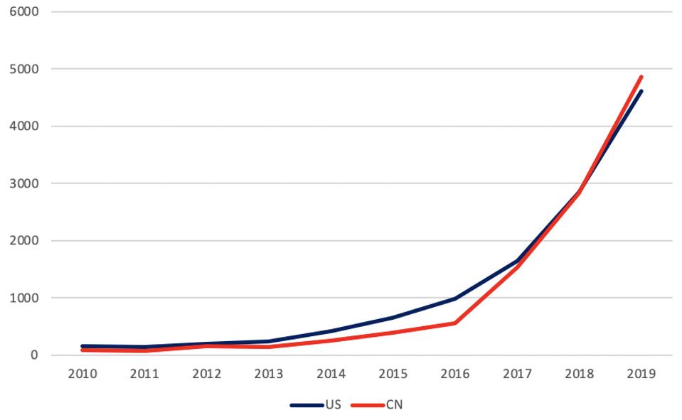
While software development is critical for the advancement of AI systems, specialized hardware is perhaps even more essential to ensuring that the software can provide results in a timely and comprehensive fashion. The chart below shows the progression of patent innovations published in the area of specialized AI chip development between the U.S. and China in the past ten years. China has been keeping pace with the U.S. in terms of patent innovations published per year during that time—and in 2019, it passed the U.S. for the first time.
AI hardware patenting trends from the US and China - data provided by Clarivate Analytics
Patinformatics, LLC
On August 28, China revised its list of banned or restricted technologies for export from the country for the first time in 12 years and AI was on the list. Even before the restrictions, China had made the development of AI systems a national imperative and China’s State Council published a policy blueprint in the summer of 2017 that set out the goal of creating the “world’s primary AI innovation center” by 2030. The plan included ambitious goals for software development, but also covered the importance of chip development, especially chips that could be used in mobile devices. A great deal of research was carried out at the Chinese Academy of Sciences, but it’s two graduates of this university system that are making the biggest waves in the AI chip market.
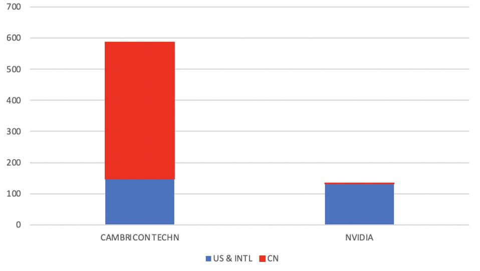
Brothers Yunhi and Tianshi Chen are the brains behind Cambricon Technologies, the company providing hardware for China’s AI ambitions. Cambricon is valued at $2.5 billion and recently raised $368 million in its IPO. The company’s Cambricon-1H and Cambricon-1M chips can already be found in almost 100 million mobile devices and servers. Its flagship Cambricon-1A is used in edge devices and has been touted as the first deep learning processor for commercial use. Besides having chips that are powering servers for Alibaba and Huawei’s latest generation of AI-enabled smartphones, the company also has one of the largest patent portfolios in the field. The graph below compares the size of the Cambricon AI chip patent portfolio to Nvidia’s. The U.S. company is considered one of the leaders in the AI chip field with its Ampere AI chip.
Count of AI hardware patents from Cambricon and Nvidia - data provided by Clarivate Analytics
Patinformatics, LLC
Chinese companies are criticized for only filing patents in their home country and this leads to some speculation about how valuable these patent filings are. As seen in the graph above, Cambricon is a notable exception to these criticisms, since a substantial portion of its portfolio is made up of patents filed for in the U.S. or using the World Intellectual Property Organization international application. Even if Chinese patent filings weren’t included—and they most certainly should be—Cambricon would still have more U.S. and international filings in this area than Nvidia. The U.S. company does have a larger patent portfolio than Cambricon overall, but only a portion of it covers AI acceleration hardware.
AI hardware or chipsets are specialized microprocessors that are designed to accelerate AI software systems. For example, these customized chipsets are meant to increase the performance of artificial neural networks. Training and implementing of these systems require vast amounts of data and hardware that can process it in parallel while maintaining low power demands. Early AI chip implementations relied on general-purpose GPUs, but recent research has gone into the invention of hardware exclusively designed for running AI software.
So far, Chinese companies have been happy with feeding the growing needs of the Chinese market for AI hardware. This fits with the national imperative to become the world’s innovative leader in this technology. At some point however, as the need for AI systems grow globally, Chinese organizations may look to expand into these markets as well.
The Chinese government’s new export restrictions will make that even more challenging. Cambricon and its brethren have a home field advantage in China, but will face an uphill struggle to overcome not only internal restrictions but foreign constraints such as the ones Huawei has encountered with Western governments. Chinese companies have an advantage with the stockpile of patents they’ve generated, but it remains to be seen if they can translate this into a stunning commercial success.
The chip industry is making progress in multiple physical dimensions and with multiple architectural approaches, setting the stage for huge performance increases based on more modular and heterogeneous designs, new advanced packaging options, and continued scaling of digital logic for at least a couple more process nodes.
A number of these changes have been discussed in recent conferences. Individually, they are potentially significant. But taken as a whole, they point to some important trends as the benefits of device scaling dwindle and market needs change. Among them:
For high-performance applications, chips are being designed based upon much more limited data movement and near-memory computing. This can be seen in floor plans where I/Os are on the perimeter of the chip rather than in the center, an approach that will increase performance by reducing the distance that data needs to travel, and consequently lower the overall power consumption.
Scaling of digital logic will continue beyond 3nm using high-NA EUV, a variety of gate-all-around FETs (CFETs, nanosheet/nanowire FETs), and carbon nanotube devices. At the same time, reticle sizes will increase to allow more components to fit into a package, if not on a single die. Both moves will add substantially more real estate by shrinking features, allowing for greater compute density. In addition, scaling of SRAM will continue, and more layers will be added for high-bandwidth memory (HBM) modules and for 3D-NAND flash.
Designs are becoming both more modular and more heterogeneous, setting the stage for more customization and faster time to market. All of the major foundries and OSATs are now endorsing a chiplet strategy, and they are offering multiple options based upon price and performance requirements.
Some of this has been in the works for years, but much of the development has been piecemeal. There is no single industry roadmap anymore, which in the past has been used as a guide for how all the developments fit together. Work continues on all fronts in the absence of that roadmap, but it frequently is difficult to understand how the big picture is developing because not everything is moving in sync. For example, ASML was talking publicly about high-numerical aperture EUV, which replaces a flat lens with an anamorphic one, even before EUV was commercially viable. And companies such as ASE and Amkor have been working on multiple versions of fan-outs, 2.5D and 3D-ICs for the better part of this decade, even though the market for these packaging schemes are very different than initially thought.
There are many new developments on the horizon, as well. Major foundries such as TSMC, UMC, GlobalFoundries and Samsung are building advanced packaging capabilities into the backend of manufacturing. TSMC also is planning to add chiplets into the frontend using bump-less hybrid bonding, which it calls SoIC. All of these will likely require significant changes across the industry, from EDA tools to test and post-silicon monitoring.
How quickly all of these different elements come together is unclear. No one likes to be first, and at this point, it’s not obvious which of these approaches and technologies will win, or even whether they will compete with each other. But change is essential as the volume of data continues to grow. This is driving more customized solutions to process and utilize that data closer to the source, which includes some level of intelligence nearly everywhere.
In the past, solutions were developed around the most advanced hardware or software based on the assumption that the next process generation would add big improvements in performance. That no longer works. Scaling is becoming more difficult and expensive, and power/performance benefits of shrinking features are diminishing. In addition, one size no longer fits all. It can vary greatly depending upon where end customers are in the compute hierarchy — end point, edge, or cloud — and how data needs to be structured and prioritized. As a result, chipmakers have shifted their focus to new and more modular architectures that are capable of everything from massive simulations and training algorithms in the cloud, to weeding out useless image and streaming video data at the source.
Put in perspective, more processing needs to happen everywhere faster, and it needs to be done using the same or less power. In addition, systems need to be created faster, and they need the ability to change much more quickly as market needs evolve and algorithms continue to change.
Architectural shifts
To make that happen, hardware architectures need to change. Chipmakers have seen this coming for some time. For example, IBM’s new Power 10 chip concentrates customized compute elements in the center of the chip and moves peripherals and I/O to the edges.
“Acceleration needs to get pushed into the processor core,” said Bill Starke, the chip’s chief architect, at the recent Hot Chips conference. “Around the chip perimeter are PHYs.” IBM also introduced pod-level clustering, and added a new microarchitecture to support all of this.
Fig. 1: IBM’s Power 10 chip (L., from Hot Chips 2020), with processing cores concentrated in the middle of the chip served by localized memory and shared L3, vs. Power 9 (R., from Hot Chips 2018) with off-chip interconnect in center. Source: IBM/Hot Chips 2018/20
Others are taking similar approaches. Intel introduced a new architecture based on internally-developed chiplets, which clusters modular processing elements together using its Embedded Multichip Interconnect Bridges to HBM modules. In addition, it has updated its latest server chip architecture to minimize data movement.
Fig. 2: Intel’s latest server processor architecture (R.) reduces movement of data compared to the previous generation (L.) Source: Intel/Hot Chips
Likewise, Tenstorrent, which makes AI systems, created a highly modular system that includes 120 self-contained cores connected with a 2D bi-directional torus NoC. “Every core progresses at its own pace,” according to Jasmina Vasiljevic, director of software engineering at Tenstorrent.
Scaling continues
Data center chips are far less cost-sensitive than in consumer applications, so they tend to lead the industry in performance. A high-performance server amortizes chip development costs with the price of a system rather than through volume, which is essential for a mobile phone application processor, for example. So despite a never-ending stream of predictions about the end of Moore’s Law, the digital logic inside many of these devices will continue to use the latest process geometries for density reasons.
What’s different, though, is less performance-critical circuitry, as well as analog blocks, increasingly is being shunted off to separate chips, which are connected using high-speed interfaces.
“You now can partition by node,” said Matt Hogan, product director at Mentor, a Siemens Business. “So you can determine what is the correct technology for a particular portion of a design. That also allows you to scale some of the side effects.”
This approach was mentioned by Gordon Moore when he first published his now-famous observation in 1965.
“With the rapid evolution of process technology, it was typically cheaper to go with an off-the-shelf solution instead of developing custom chips,” said Tim Kogel, principal applications engineer at Synopsys. “By now, the free lunch of higher performance and lower power with every new process node is all but over. On the other hand, killer applications like AI, autonomous driving, AR/VR, etc., have an unquenchable demand for processing power and computational efficiency. Famous examples like Google’s TPU and Tesla’s FSD chips show the impressive ROI of tailoring the architecture to the specific characteristics of the target workload.”
Still, the value of Moore’s Law as originally written is waning, and that has both economic and technological implications. The economic benefits of planar scaling ended with the introduction of finFETs, when cost per transistor stopped decreasing from the previous node. Likewise, power/performance benefits have been decreasing since about 90nm. Y.J. Mii, senior vice president of R&D at TSMC, said that 3nm will bring performance improvements of just 10% to 15% for the same power, or 25% to 30% power reduction for the same speed.
This is hardly a dead end from a technology standpoint, however. Architectural improvements, including different packaging approaches and 3D layouts, can boost that performance by orders of magnitude. And scaling still helps to pack more density into those packages, even if the scaled-down transistors themselves aren’t running significantly faster.
“We have been bombarded by More-than-Moore topics for many years now,” said Tom Wong, director of marketing for design IP at Cadence. “But is it really area reduction, power reduction or transistor performance improvements (traditional PPA) that are driving these discussions, or is it silicon economics and the limitations of lithography/equipment that caused us to hit the brick wall? As it turns out, silicon economics and the limits of reticle size are the two things driving a disruption, which is necessitating designers to look at new ways of designing chips, and turning to new architectures.”
Both economics and reticle size limits are being addressed through different packaging schemes and a boost in reticle sizes, which allow for much bigger individual die. Doug Yu, vice president of R&D at TSMC, said that reticle sizes will increase by 1.7X with the foundry’s InFO (integrated fan-out) packaging approach. In addition, TSMC plans to introduce a 110 x 110 mm² reticle in Q1 of next year, which will increase reticle size by 2.5X.
All of this is necessary as the cost of putting everything onto a single die continues to rise. Modularity allows chipmakers to customize chips relatively quickly based upon a platform type of approach. CPU, GPU and FPGA chip designers figured this out more than five years ago, and have since started the march to disaggregated implementation by going to multi-die, and letting the interposer/packaging take care of the integration. This is one reason why die-to-die connectivity IP is taking center stage today, Wong said.
“CPUs, GPUs and FPGAs have all gone the route of chiplets because these companies design the chips (chiplets) themselves and need not rely on a commercial chiplet ecosystem. They can take advantage of what a chiplet-based design can offer,” Wong noted. “Multi-core designs, including CPUs, GPUs and FPGAs, can benefit from this architectural change/trend. SoC designs that can separate ‘core compute’ and high-speed I/Os also can benefit from this. AI acceleration SoCs and crypto SoCs are two examples. And datacenter switches and fabrics, such as 25.6Tb/s for hyperscale compute and cloud builders, also can benefit from this architectural change to chiplet-based design. These designs can be as complex as 20 billion+ transistors.”
So far this approach has been utilized by IDMs such as Intel, AMD and Marvell, each creating its own modular schemes and interconnects. So rather than building a chip and trying to pitch its benefits across a broad range of customers, they offer a menu of options using chiplets and, in Intel’s case, an assortment of connectivity options such as high-speed bridges.
Changes everywhere, some big, some tiny
Putting all these changes into perspective is often difficult because the whole industry is in motion, although not necessarily at the same velocity or for the same reasons. So while processors and processes change, for example, memory lags well behind.
In addition, some technologies need to be completely rethought while others stay the same. This is particularly evident with GPUs, which have been the go-to solution for AI/ML training because they are cheap and scalable. But they are not the most energy-efficient approach.
“We’ve seen it with bandwidth, we’ve seen it with power,” said Kristof Beets, senior director of product management and technology marketing at Imagination Technologies “All of these different constraints come into play. From a GPU point of view it’s been a tricky evolution, because obviously GPUs are massive number crunchers, displays get ever bigger, and devices get ever smaller. So a lot of these problems keep hitting. There’s been a phase of brute force, which kind of depended on Moore’s Law. We were doubling the GPU, and for a while that was okay, because process technology kept up. But now that return is diminishing, so while we can put more logic down, we basically can’t turn it on anymore because it consumes too much power. So the brute force trick doesn’t work.”
Dynamic voltage and frequency scaling (DVFS) has helped a bit to ramp down the voltage, allowing for even bigger GPUs running at lower frequencies. Nevertheless, even that approach has limits because there are only so many GPU cores that can be used within a fixed power budget. “This gives us better FPS (frames per second) per watt, but even that is now starting to slow because leakage is going up again,” Beets said. “This is where, for GPUs, ray tracing has been interesting. It’s a way of switching away from brute force. They are very flexible. We’re seeing the same with AI and neural network processing. It’s exactly the same concept. This is where you’ve truly seen orders of magnitude solutions that are 10, 20 times better than the GPU by taking into account the data flow, the specific operations, so it’s quite interesting. It’s not quite as bad as the old days of fixed function processing. We’re not back there yet. But some of it is definitely starting to return with more dedicated processing types.”
There are many approaches to augmenting scaling performance. “There have been a few areas, such as application processors, GPUs, MCUs, DSPs, where we’ve had fairly general-purpose architectures exploiting Moore’s Law to do more and more,” said Roddy Urquhart, senior marketing director at Codasip. “But now there are a huge number of ideas around trying out novel architectures, novel structures, with a range of programmability. At the systolic array end, there are things that tend to be either hardwired processing elements, or they have processes that have firmware uploaded and left in a static condition for some time. At the other extreme are domain-specific processes, which are highly programmable. I see a return to innovation in the highly parallel, highly pipelined, array-type structures, which is a very good fit with neural networks of different sorts. At the other end, people are thinking more outside the box for moving out of the silos of MCU, GPU, DSP and application processors, and creating something that is more of a blended version of some of these things to meet particular needs.”
Micro-architectures
Alongside of these broad architectural shifts are micro-architectural innovations. In many respects, this is a partitioning problem, where some compute functions are given priority over others within a larger system. That can have a big impact on both performance and computational efficiency.
“Taking advantage of the inherent parallelism, the application should be mapped to an optimal set of heterogenous processing elements,” said Synopsys’ Kogel. “Choosing for each function a processing core that provides the minimum required flexibility gives the highest possible computational efficiency. Also, the organization of the memory architecture has a very high impact on performance and power. Since external memory accesses are expensive, data should be kept in on-chip memories, close to where it is processed.”
This is easier said than done, however, and it requires multi-disciplinary and, increasingly, multi-dimensional planning. “It’s quite a challenge to manage the complexity and predict the dynamic effects of a highly parallel application running on heterogenous multi-processing platform with distributed memories,” Kogel said. “We propose the use of virtual prototyping to quantitatively analyze architecture tradeoffs early in the development process. This enables the collaboration of stakeholders from application and implementation teams, before committing to an implementation specification.”
New tradeoffs
Going forward, how to proceed with power and performance tradeoffs depends on the market. Some markets are highly cost-sensitive, so they haven’t ramped into this problem yet. At the same time, others are less cost-sensitive and more latency-sensitive.
“People are increasingly impatient. You want to get stuff that you want as quickly as possible,” said Mike Mayberry, CTO of Intel, during a panel presentation at DARPA’s recent Electronics Resurgence Initiative (ERI) Summit. “But we’re also seeing balanced systems and more compute near the data, and that’s one of the trends we see continuing.”
Mayberry noted there is no hard stop on density scaling, but increasingly it will include the Z axis. “We’re also seeing novel beyond-CMOS devices that will enable heterogeneous architectures. A decade from now, you’ll see those on shelves.”
Intel, among others, is looking at ways to grow devices in addition to depositing and etching different materials. This has been talked about for years with such approaches as directed self-assembly. At some point that still may be economically viable, but the general consensus is probably not until after 3nm.
Alongside of all of this, photonics is beginning to gather some momentum as a way of moving large quantities of data in and around these increasingly dense structures with minimal heat. One of the more novel approaches involves using light for processing, which LightMatter CEO Nick Harris said is free from effects like time-dependent dielectric breakdown because it doesn’t rely on transistors. What’s particularly unique about this approach is that light can be partitioned into different wavelengths, allowing different colors to be given different prioritization.
“With 100GHz wavelengths, which is really small spacing, we can fit 1,000 colors,” Harris said. The downside is lasers don’t last forever, so there needs to be enough redundancy to allow these systems to last throughout their expected lifetimes.
For more traditional computing, the number of process node options is increasing, as well. Foundries are offering in-between nodes, which improve performance or power without a complete redesign. For example, TSMC uncorked its N4 process, which will enter risk production at the end of next year. C.C. Wei, CEO of TSMC, said in a presentation that IP used in both N5 (5nm) and N4 will be compatible, which allows companies to improve density and lower power with minimal redesign.
Still, the number of options is dizzying. In addition to different node numbers, there also are different process options for low power and for high performance. On top of that, different substrate materials are beginning to gain traction, including silicon carbide and gallium nitride for power transistors, and silicon-on-insulator for lower-cost, low-power applications.
All of that has a big impact on design rules, which are used to prevent failures. “If you’re designing a chiplet, you don’t know how it’s going to be used or placed,” said Mentor’s Hogan. “You don’t know if it’s going to be next to an MCU, so you have to figure out how to do that in a thoughtful way. You need to protect it from electromagnetic effects and other potential issues.”
And because chips are expected to function properly for longer periods of time — in the case of automotive, it may be as long as 18 years for leading-node logic — all of this needs to be done in the context of aging. This can get extremely complicated, particularly in multi-chip packages.
“You need to look at things like threshold shifts with different stimuli and scenarios,” said Vic Kulkarni, vice president of marketing and chief strategist for the semiconductor business unit at Ansys. “You can do a precise analysis of registers, but if the Vdd is not going down and the Vt is not going down, there isn’t much margin left. You also need to think about things like electrical overstress. The fabs are not willing to take that on.”
Tradeoffs range from power, performance, and cost, to quality of service.
“We used to always have lossless compression,” said Imagination’s Beets. “And about one or two years ago, we introduced lossy, as well, so we could trade off on quality. In GPUs, we’re starting to see across the board a tradeoff of quality versus cost, and the lossy compression allows the quality to be decreased, which also saves on bandwidth and power. In GPU processing, we’re starting to see the same thing, which is variable rate shading. This is basically when you look at a video, you’d say all you really care about is the face, and you want that in full detail, so the background doesn’t matter. Games essentially do the same thing. For example, in a racing game the car is very sharp and has a lot of detail, but the rest has a motion blur on it.”
There also are tradeoffs in precision. Lower precision can greatly speed up processing, and sparser algorithms can be written to be less precise, whether that’s 16-bit precision or even 1-bit precision. But that precision also can be controlled by the hardware and firmware, and it can have a big impact on overall system performance where some functions are made more accurate than others.
Conclusion
For the first 40 years or so of Moore’s Law, power, performance and area improvements were sufficient for most applications, and the growth in data generally was manageable through classical scaling. After 90nm, classical scaling started showing signs of stress. So the writing has been on the wall for some time, but it has not gone unheeded.
What’s surprising, though, is just how many avenues are still available for massive improvements in performance, lower power and potentially cost savings. Engineering teams are innovating in new and interesting ways. Decades of research into what seemed like obscure topics or tangents at the time are now paying off, and there is plenty more in the pipeline.
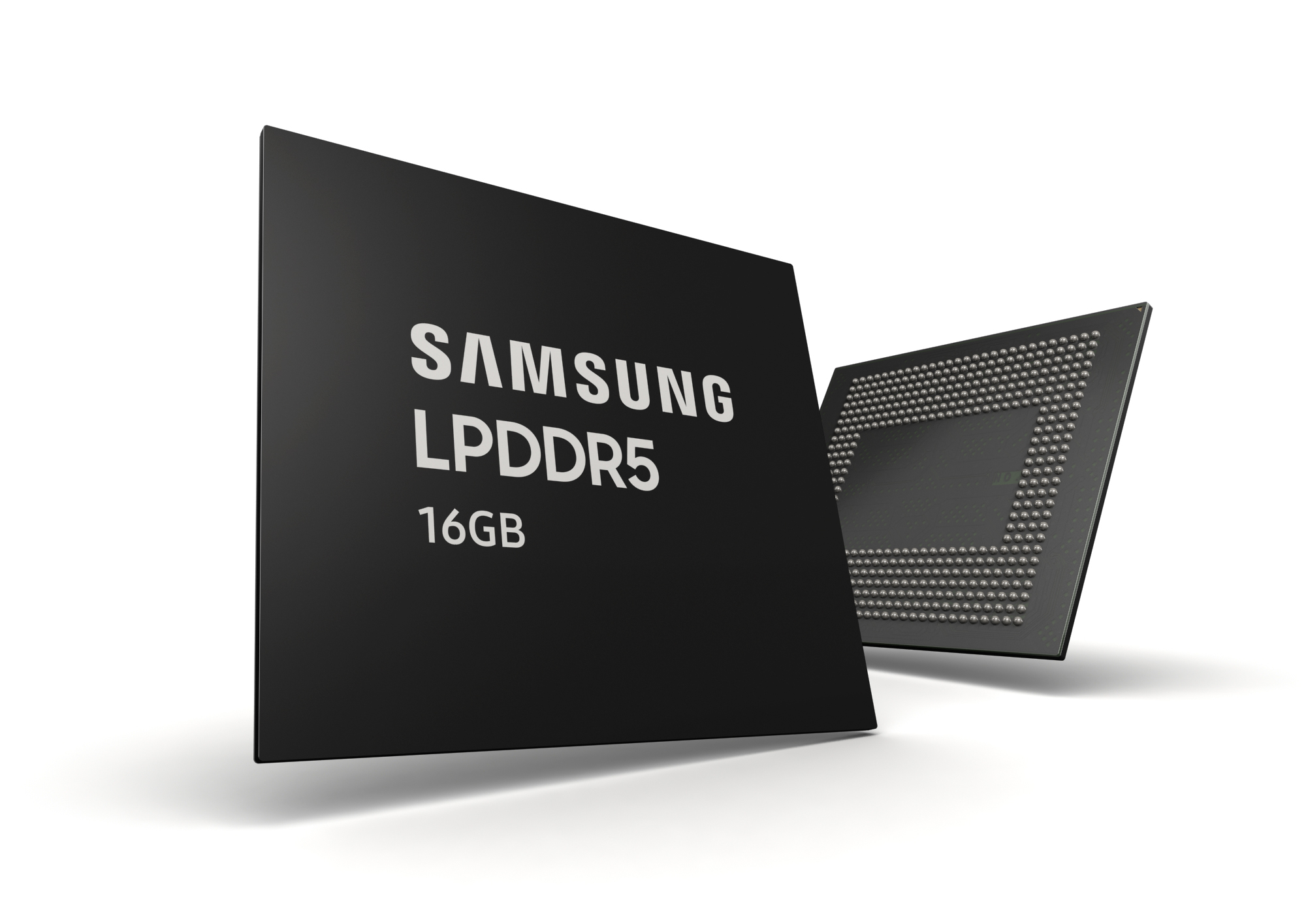
Samsung Electronics Co. Ltd. said today it has begun mass production of its most advanced dynamic random-access memory chips yet.
The 16-gigabyte LPDDR5 DRAM chip is designed for mobile devices and is being manufactured at the company’s Pyeongtaek plant in South Korea, using a new process called extreme ultraviolet lithography. That process involves using lasers and light-sensitive chemicals to etch silicon, and overcomes a “major developmental hurdle” in scaling RAM, providing much greater room for the industry to grow.
The South Korean tech giant is the leader of the global DRAM market, and the advent of the new chips makes it likely that the company will be able to extend that lead. It’s an important market for Samsung too, since the memory chip business accounts for about two-thirds of its overall revenue, dwarfing other businesses such as its smartphone unit and its household appliance division.
Samsung said the EUV manufacturing process results in a chip that is 30% thinner than its previous-generation chips. But despite the smaller size, the chips are also faster, averaging data transfer rates of 6,400 megabits per second. That means it can send 51.2GB of data, or the equivalent of 10 5GB movies, in just a second.
“The 1z-based 16Gb LPDDR5 elevates the industry to a new threshold, overcoming a major developmental hurdle in DRAM scaling at advanced nodes,” said Jung-Bae Lee, executive vice president of DRAM Product & Technology at Samsung. “We will continue to expand our premium DRAM lineup and exceed customer demands, as we lead in growing the overall memory market.”
Samsung said it will combine eight of the new chips to form a 16GB RAM package that’s intended for the next generation of premium smartphones due to arrive in 2021. The smaller size of the chips will mean either slimmer smartphone designs or more room for other components such as batteries and cameras. In addition, new smartphones based on the 16GB LPDDR5 will have more significantly more headroom for running simultaneous apps and performing more demanding tasks.
Samsung is also eyeing the automotive industry, where the new chips could be used to power faster and more powerful infotainment systems.
Image: Samsung
Since you’re here …
Show your support for our mission with our one-click subscription to our YouTube channel (below). The more subscribers we have, the more YouTube will suggest relevant enterprise and emerging technology content to you. Thanks!
… We’d also like to tell you about our mission and how you can help us fulfill it. SiliconANGLE Media Inc.’s business model is based on the intrinsic value of the content, not advertising. Unlike many online publications, we don’t have a paywall or run banner advertising, because we want to keep our journalism open, without influence or the need to chase traffic.The journalism, reporting and commentary on SiliconANGLE — along with live, unscripted video from our Silicon Valley studio and globe-trotting video teams at theCUBE — take a lot of hard work, time and money. Keeping the quality high requires the support of sponsors who are aligned with our vision of ad-free journalism content.
If you like the reporting, video interviews and other ad-free content here, please take a moment to check out a sample of the video content supported by our sponsors, tweet your support, and keep coming back to SiliconANGLE.
In this year of uncertainty, do you find yourself settling into certain habits or routines? In many circumstances, we’re hardwired to embrace behavior that’s comfortable or safe. We like what we know.
Habits and routines are often mentioned interchangeably, but they’re different. A habit is an action that’s done automatically. Do you keep your car keys in the same location when you walk into the house?
A routine is a sequence of actions done repeatedly. A regular morning exercise, brushing your teeth, waking up early. Those daily repeated routines trigger the beginning of a day.
Not all habits or routines are productive or good for us.
I have this issue with potato chips. A televised ballgame, my recliner, a bag of chips. There’s a synergy that develops here on an all too frequent basis. As a matter of fact, it appears that habit has developed into a routine.
Some folks aren’t able to start the day without the necessary cup of coffee. We once programmed the coffeemaker before going to bed. These days, we’ve progressed to the individual cups that better suit particular tastes. The routine has been altered, but the habit of needing the kick-start remains.
A proper breakfast also is recommended to routinely begin each day. Oatmeal or yogurt are suggested in order to avoid foods high in sugar or fat. Unfortunately, my routine often involves a drive-thru window and a country ham biscuit.
Creatures of habit
Do you make your bed every day? I’ve read that some behavior experts feel this is an extremely important habit to include in your routine. It provides an immediate, small sense of accomplishment. It also signifies a completion of the first task of the day that subliminally signals that in life, little things matter.
I would put myself somewhere in the 75 to 78 percentile on the chart of regular bed-making. Maybe that’s why, some days, I feel more productive than others.
Sign up for our new opinion newsletter
Get a weekly recap of South Carolina opinion and analysis from The Post and Courier in your inbox on Monday evenings.
As far as other matters around the house, there are some I’m still trying to better understand. For instance, I’m not sure why it’s important to clean up the house before the person coming to clean the house arrives. I’m also a bit confused why the dishes have to essentially be cleaned before placing them in the dishwasher.
My guess is that there are a few of you shaking your heads in agreement and a few others of you dismissively saying you know somebody who thinks just like I do. We can sort all of this out later.
Words and actions
Our country is having a tough time right now purging itself of old habits and routines that have affected how we treat and relate to each other. The preconceived notions, the jokes or words once used freely around the dinner table are no longer acceptable.
The racial injustice versus people of color during routine encounters just can’t continue. It feels like a moment to me. A moment that all these hateful habits must change.
I understand the outrage and the frustration that continues to build when the words don’t match the actions.
If our hearts and minds don’t undergo a deep cleaning, accompanied by an even deeper understanding, how we relate and respect each other may never improve.
I suppose we can keep putting all the dirty plates into that socially flawed dishwasher until it can hold no more. But unless some extra attention is paid to individually scrubbing how we think beforehand, the habits and old routines will never be washed away.