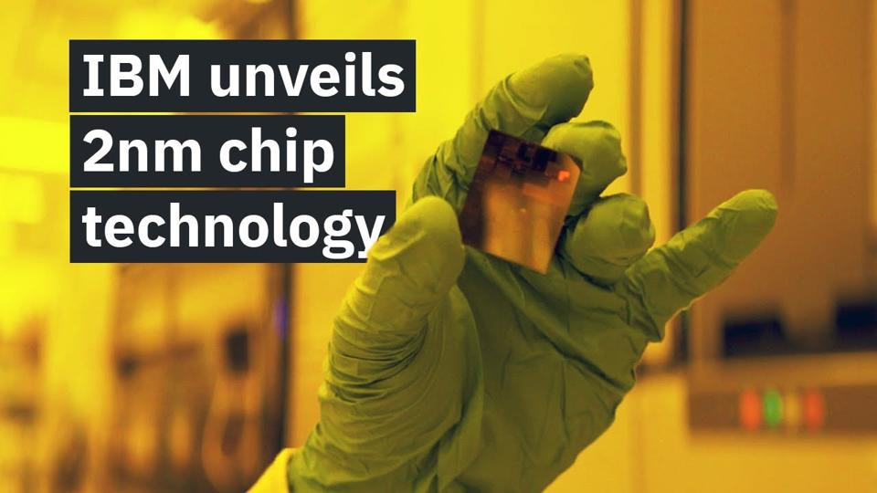
IBM unveils 2nm Chip Technology
IBMA fact of life in the tech industry is that you can never stay still. It’s a never-ending arms race, with businesses big and small attempting to outpace each other for a piece of the pie. The highly competitive semiconductor sector has seen several pieces of big news over the last month, both involving industry mainstay IBM. First, IBM announced a surprise partnership with Intel (historically, an IBM competitor) to research new logic and packaging technologies. This past week, IBM kept itself in the headlines with another big reveal: the world’s first test chip utilizing 2nm technology. In an industry where everyone is always looking to build smaller, faster and more efficiently, this news represents a significant breakthrough. Let’s take a look at the details.
A next level chip for next-level applications
Semiconductors function essentially as the “brain” inside of our intelligent devices. We depend on these pieces of silicon daily, as they show up in our computers, phones, appliances, vehicles and virtually anywhere else computation happens. The major chipmakers have been in a shrink-off with each other over the packaging technology used to build these chips for years. IBM has proven itself a standout time and time again, with the distinction of debuting the first 5nm, 7nm and 10nm test chips on the market. IBM’s first 7nm chip, Power10, was unveiled last year.
Each incremental reduction in size translates to significant improvements in performance and efficiency—key to unlocking the full potential of ascendent technologies like hybrid cloud, Artificial Intelligence (AI) and the Internet of Things (IoT). To put some numbers on it, IBM projects that the new 2nm chip will best perform today’s leading 7nm offerings by as much as 45% or utilize 75% less energy.
IBM also shared some specific potential use cases for 2nm. Amongst other things, these advances could theoretically:
- quadruple the life of a cell phone battery
- give laptop processing a kick in the pants, enabling faster internet speeds, real-time language translation, and more
- allow the lightning-fast object detection and reaction time necessary for safe autonomous vehicles.
MORE FOR YOU
Also worth mentioning is that 2nm chips could be a real game-changer in the data center, where IBM is already a heavyweight with its Power line of processors. Data centers account for a significant 1% of all global energy use, and 2nm’s energy efficiency could drastically reduce their collective massive carbon footprint.
Several additional key innovations
The development of 2nm tech has yielded several other critical technological advancements. For one, it represents the industry’s first instance of bottom dielectric isolation. This technology ensures the 2nm transistors can continue to switch on and off as they scale up. This, IBM believes, makes it possible to eliminate current leakage from the nanosheets that make up 2nm technology. Additionally, IBM highlighted both a new inner spacer process, which gives the chip more precise gate control and the world’s first UV brightening on the front end. IBM has employed the latter tech since its 7nm breakthrough, but historically it has been relegated to the middle or back end.
Wrapping up
IBM has shown, yet again, that it is a leader in semiconductor research and development—not surprising given the emphasis it puts on this critical part of its business. Its vast ecosystem now includes over 300 research labs worldwide, including the state-of-the-art R&D facility headquarters in Albany, where IBM made the 2nm breakthrough. With these resources at IBM’s disposal, it’s no wonder the company continues to expand the limits of what’s possible in chipmaking. I can’t wait to see what IBM does next.
Note: Moor Insights & Strategy writers and editors may have contributed to this article.
Moor Insights & Strategy, like all research and analyst firms, provides or has provided paid research, analysis, advising, or consulting to many high-tech companies in the industry, including 8x8, Advanced Micro Devices, Amazon, Applied Micro, ARM, Aruba Networks, AT&T, AWS, A-10 Strategies, Bitfusion, Blaize, Box, Broadcom, Calix, Cisco Systems, Clear Software, Cloudera, Clumio, Cognitive Systems, CompuCom, Dell, Dell EMC, Dell Technologies, Diablo Technologies, Digital Optics, Dreamchain, Echelon, Ericsson, Extreme Networks, Flex, Foxconn, Frame (now VMware), Fujitsu, Gen Z Consortium, Glue Networks, GlobalFoundries, Google (Nest-Revolve), Google Cloud, HP Inc., Hewlett Packard Enterprise, Honeywell, Huawei Technologies, IBM, Ion VR, Inseego, Infosys, Intel, Interdigital, Jabil Circuit, Konica Minolta, Lattice Semiconductor, Lenovo, Linux Foundation, MapBox, Marvell, Mavenir, Marseille Inc, Mayfair Equity, Meraki (Cisco), Mesophere, Microsoft, Mojo Networks, National Instruments, NetApp, Nightwatch, NOKIA (Alcatel-Lucent), Nortek, Novumind, NVIDIA, Nuvia, ON Semiconductor, ONUG, OpenStack Foundation, Oracle, Poly, Panasas, Peraso, Pexip, Pixelworks, Plume Design, Poly, Portworx, Pure Storage, Qualcomm, Rackspace, Rambus, Rayvolt E-Bikes, Red Hat, Residio, Samsung Electronics, SAP, SAS, Scale Computing, Schneider Electric, Silver Peak, SONY, Springpath, Spirent, Splunk, Sprint, Stratus Technologies, Symantec, Synaptics, Syniverse, Synopsys, Tanium, TE Connectivity, TensTorrent, Tobii Technology, T-Mobile, Twitter, Unity Technologies, UiPath, Verizon Communications, Vidyo, VMware, Wave Computing, Wellsmith, Xilinx, Zebra, Zededa, and Zoho which may be cited in blogs and research
The Link LonkMay 10, 2021 at 10:50PM
https://ift.tt/3eBfQ1K
Big Blue Goes Tiny With World’s First 2nm Chip Tech - Forbes
https://ift.tt/2RGyUAH
Chips

No comments:
Post a Comment